基于开关电容技术的FM解调处理电路设计
来源:56doc.com 资料编号:5D26712 资料等级:★★★★★ %E8%B5%84%E6%96%99%E7%BC%96%E5%8F%B7%EF%BC%9A5D26712
资料以网页介绍的为准,下载后不会有水印.资料仅供学习参考之用. 密 保 惠 帮助
资料介绍
基于开关电容技术的FM解调处理电路设计(论文15000字)
摘要:针对目前FM模拟解调器自身受限于模拟体制,难以对解调后的语音信号进行滤波、分析处理等问题,本系统设计出了一种基于开关电容技术的FM解调处理电路。开关电容滤波器可以通过改变时钟信号频率,利用时钟信号频率和滤波器中心频率和Q值的固定关系,快捷方便地改变滤波器的幅频特性,而无需像传统有源或无源滤波器一样需要根据实际要求频繁更换电子元件。本设计利用锁相环鉴频法对FM波进行解调,将解调后的信号通过波形变换、倍频处理后自动产生开关电容滤波器时钟信号,并将该时钟信号输送给开关电容滤波器,对解调后的信号自动进行滤波操作。该系统利用硬件电路实现自适应滤波,经实验证明具有较高的可靠性。
关键词:滤波器、开关电容技术、解调处理、FM波
FM Demodulation Processing Circuit Based on Switched Capacitor Technology
Abstract:In this design, a FM demodulation circuit based on switched capacitor technology is designed to solve the problem that FM analog demodulator that is limited by analog system and it is difficult to filter and analyze the demodulated speech signal. The greatest advantage of switched capacitor filter in application is that it does not need to replace components, only to change the clock frequency and programming pin level by changing the central frequency and Q value of the filter in a certain range, which brings great convenience to the design and use of the filter. In this design, FM wave is demodulated by PLL frequency discrimination method. The clock signal is automatically generated by waveform transformation and frequency multiplying of the demodulated signal, and then be transmitted to the switched capacitor filter. Finally, the demodulated signal is automatically filtered. The system uses hardware circuit to realize adaptive filtering. The experiment proves that the system has high reliability.
Key words:switch capacitor technology, filter, frequency modulation wave, demodulation processing
目 录
1 前言 1
1.1 课题背景与现状 1
1.2 目的与意义 2
2 设计原理 3
2.1 锁相鉴频原理 3
2.1.1 鉴频原理 3
2.1.2 锁相原理 3
2.1.3 锁相鉴频原理 4
2.2 波形变换和整形原理 4
2.3 锁相环倍频原理 4
2.4 开关电容滤波器(SCF)原理 5
3 设计过程 6
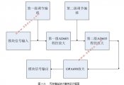
3.1 系统设计框图 6
3.2 锁相鉴频器 7
3.2.1 NE564 7
3.2.2 CD4046的特点和基本组成 8
3.2.3 NE564和CD4046的选择 10
3.3 波形变换和整形电路 10
3.3.1 滞回比较器和电平转换组合 10
3.3.2 施密特触发器 11
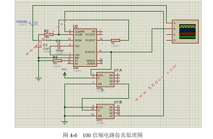
3.4 100倍频电路 13
3.4.1 利用FPGA内部锁相环实现100倍频 13
3.4.2 用锁相环和分频器组成100倍频模块 13
3.4.3 写Verilog 100倍频程序 14
3.4.4 傅里叶法倍频 14
3.4.5 参量法倍频 14
3.5 开关电容滤波器(SCF) 15
3.5.1 MAX26X系列 通用开关电容滤波器 15
3.5.2 LTC1068开关电容滤波器 16
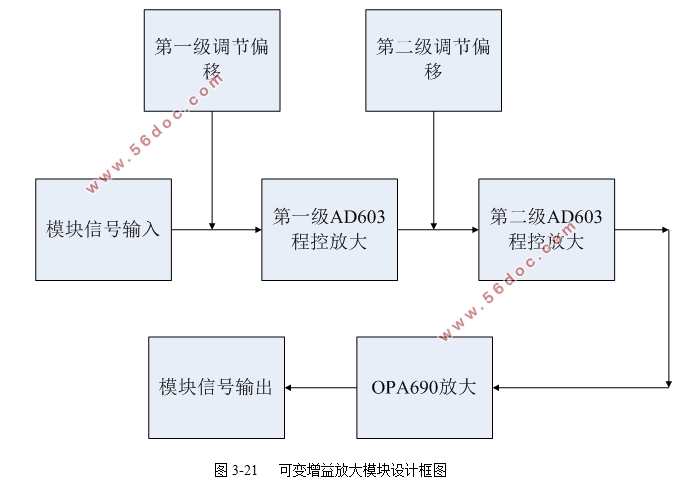
3.6 可变增益放大器 18
3.6.1 使用电位器和运算放大器构成增益可控放大电路 18
3.6.2 AD603和 OPA690的组合放大 19
3.7 直流偏置电路 21
3.7.1 分压耦合偏置 21
3.7.2 同相比例加法偏置电路 21
4 仿真和实物测试结果 22
4.1 CD4046调制解调电路仿真 22
4.2 波形变换和整形电路仿真和实物测试 23
4.2.1 仿真结果 23
4.2.2 实物测试结果 23
4.3 100倍频电路仿真和实物测试 24
4.3.1 仿真结果 24
4.3.2 实物测试结果 25
4.4 可变增益放大器仿真测试 26
4.4.1 仿真结果 26
4.4.2 实物测试结果 27
4.5 直流偏置电路仿真和实物测试 28
4.5.1 仿真结果 28
4.5.2 实物测试结果 28
4.6 系统实物图及测试结果 29
4.6.1 实物图 29
4.6.2 系统带宽测试 30
5 总结 30
参考文献 31
致 谢 33
|