基于FPGA的数字存储示波器设计
来源:56doc.com 资料编号:5D27817 资料等级:★★★★★ %E8%B5%84%E6%96%99%E7%BC%96%E5%8F%B7%EF%BC%9A5D27817
资料以网页介绍的为准,下载后不会有水印.资料仅供学习参考之用. 密 保 惠 帮助
资料介绍
基于FPGA的数字存储示波器设计(任务书,开题报告,论文16000字)
摘 要
数字示波器可以在采样一定的点数情况下,将波形信号处理后实时的保存到存储器中然后将模拟信号送到VGA中,并且对比模拟示波器相比,其优点也很多,如:输出稳定,波形可存储性,操作简易等。
本系统所设计的示波器是一个可以实时采样波形点、显示功能可调整的数字存储示波器。该示波器具有组件简单并且成本低廉等优点。本系统的开发环境是vovido2014.4,一种适用于FPGA的开发环境,可以直接用Verilog语言进行开发,环境搭建简便,误差小。可以在屏幕上显示波形时长超过一个周期。
本系统是以xc7a35tcpg236-1芯片为核心,设计的部分包括:首先是模数转换模块对输入的正弦信号进行采样,在触发条件下连续采样640点存储到存储器中,通过峰峰值、频率计算模块对存储的采样点计算频率及峰峰值,最后通过VGA显示器将波形显示出来。
关键字:数字存储示波 FPGA vovido AD模块
Design of Digital Storage Oscilloscope Based on FPGA
Abstract
The digital storage oscilloscope can display the analog signal through sampling, storage and display. And digital storage oscilloscope compared with many advantages, such as: stable output, waveform storage, easy operation, etc.
The system is to build a real-time sampling, waveform adjustable digital storage oscilloscope. The oscilloscope has the advantages of simple assembly and low cost. The development environment of this system is vovido2014.4 version, which is suitable for basys3 development board. It can directly use Verilog language development, the environment is simple and with small error. And it can display the waveform on the screen over a period of more than one cycle.
The system is based on basys3 development board as the core. The design part includes: AD module to sample an analog signal, trigger circuit according to the sampling signal to determine whether the conditions meet, meet the conditions trigger continuous sampling after a certain number of points in the ARM. Through the peak to peak value and frequency calculation module, we can calculate storage of the sampling points to calculate the frequency and peak value. Finally it will be displayed through the waveform VGA display.
Keywords: digital storage oscilloscope; FPGA; vovido; AD module
目 录
摘 要 I
ABSTRACT II
第一章 引言 1
1.1 数字存储示波器概述 1
1.2 发展现状及选题意义 2
1.3 研究内容 3
第二章 数字存储示波器方案论证 5
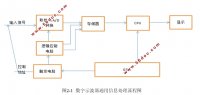
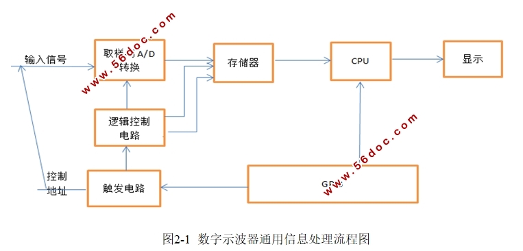
2.1 数字存储示波器的工作原理 5
2.2 示波器的技术指标 7
2.3 方案论证 8
2.4 设计方案比较与选择 9
第三章 数字示波器各模块设计 11
3.1 A/D转换模块 11
3.2 ROM模块的初始化和计算模块算法 16
3.3 VGA显示模块 18
3.4 触发电路的设计 19
3.5 峰峰值和频率计算模块 20
第四章 顶层文件的设计与实现 23
4.1 顶层文件的作用 23
4.2 设计的内容 23
第五章 系统的综合与测试结果 25
5.1 综合的作用 25
5.2 测试方案 26
5.3 测试结果 26
第六章 总结 28
参考文献 30
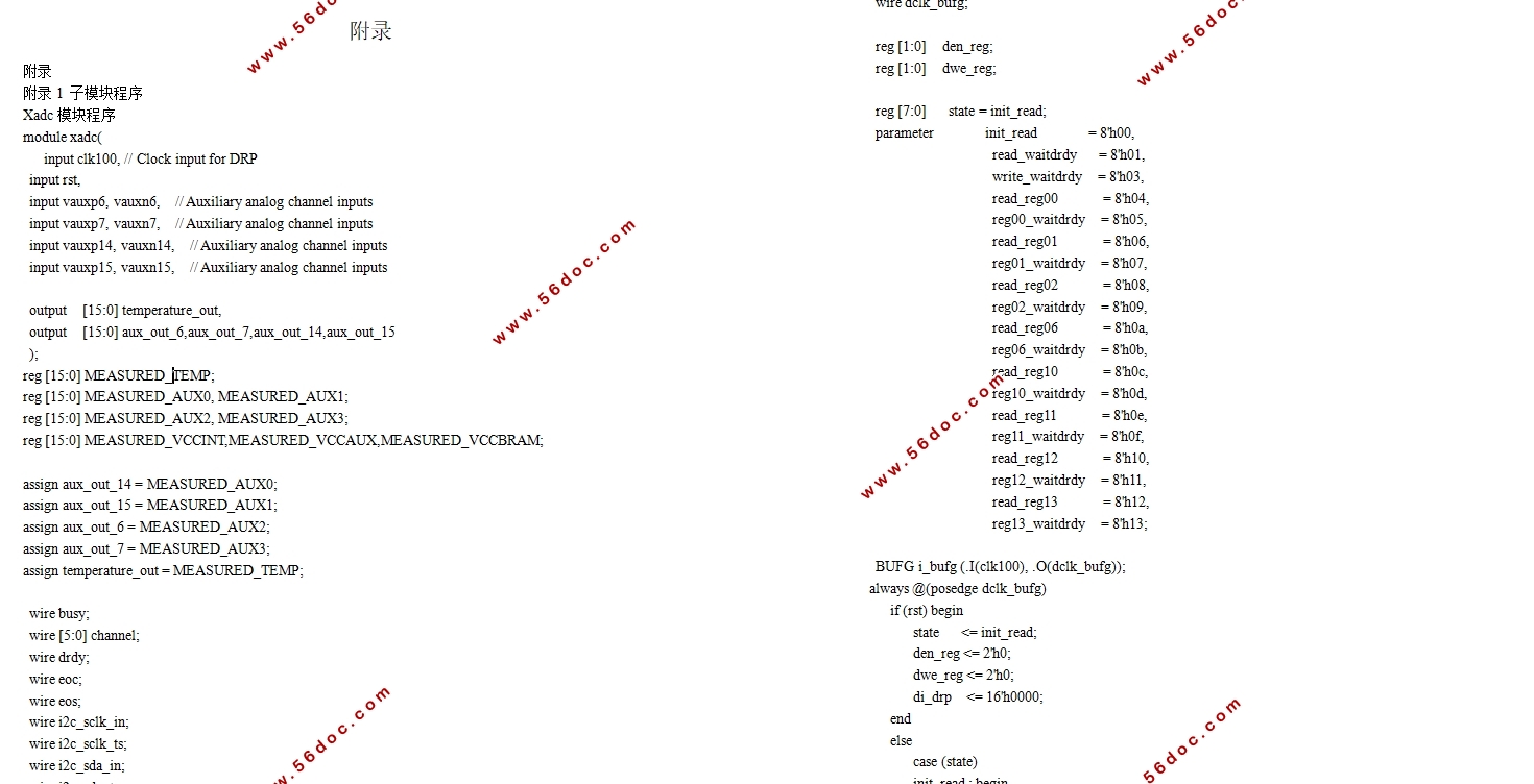
附录 32
致谢 47
|